The History of TFT (Thin Film Transistor) Displays
The History of TFT Displays
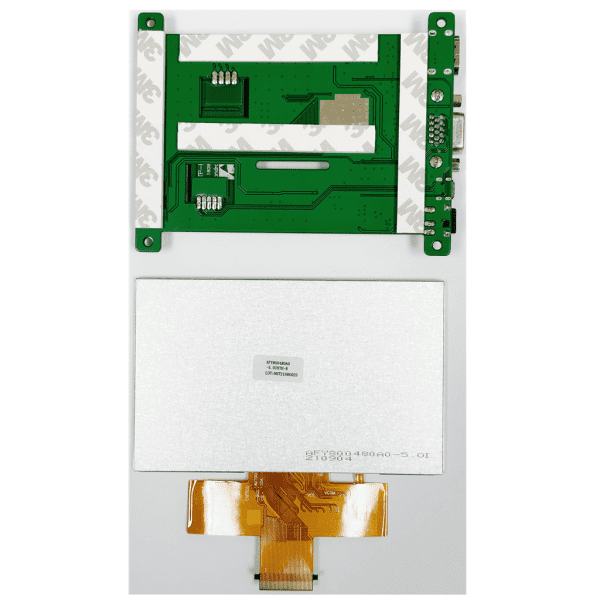
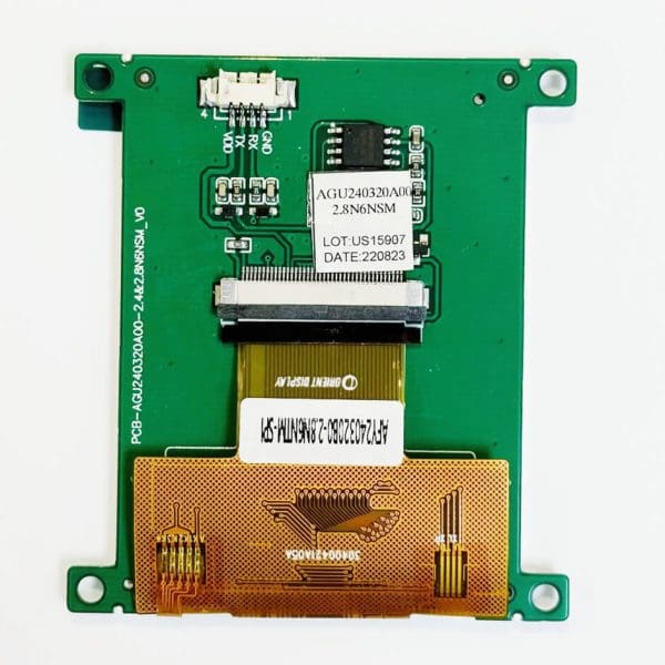
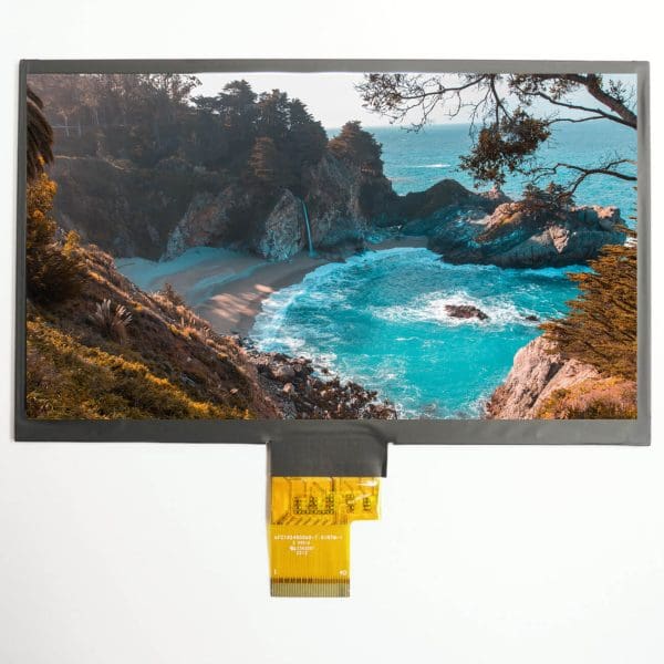
More information about TFT Technology you can find here:
As our society progresses into an overwhelmingly technological state, screens seem to pop up almost everywhere. Behind those glass displays, or flat panel displays, lie hundreds of thousands of complex, tiny devices, controlling the pixels that comprise the overall image we see. Those devices are known as Thin Film Transistors, or abbreviated, TFTs.

By Who and When was the TFT Invented?
In 1962, after a series of developments in the field of semiconductors and microelectronics, the TFT emerged. The Radio Corporation of America (RCA) had spent years experimenting and developing transistors in hopes of expanding the possibilities of their usage. Though the first thin film patent by John Wallmark (a member of the RCA) was in 1957, it was Paul K. Weimer, also from the RCA, who developed the TFT.
Evolution of TFTs
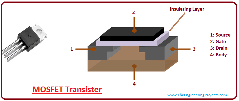
Before the emergence of the TFT, there existed the Field Effect Transistor (FET). The FET is a type of semiconductor device, allowing the transistor to have amplifying, controlling, or generating properties with electric signals. This transistor was created to control the movement and flow of current within devices. FETs have a standard build, consisting of the source, drain, and gate as well as their individual electrodes that allow for contact and conduction with the semiconductor. This device can control the applied voltage through the gate by increasing or decreasing the movement of charge carriers like electrons or holes (the absence of an electron that causes a charged pull) in a fashion called carrier mobility, or more specific to FETs, field-effect mobility. With high-mobility semiconductors, charges are more easily amplified, controlled, or generated. The FET can then alter the signals along with their strengths (from the source) sent to the destination (the drain and the designated signal recipient).
The FET was first successfully built in 1945, years after the idea was first patented in 1925. However, it was not until the experimentation that created the Metal Oxide Semiconductor Field Energy Transistor (MOSFET) many subsequent years later that the FET became much more usable. Scientists discovered that they could create a gate insulator for the device, and in doing so, it allowed for the controlled oxidation (the forced diffusion of the oxide layer into another surface) of the semiconductor piece, which has typically been made of silicon. This new layer is known as the dielectric layer or gate dielectric of the MOSFET. This development made possible the integration of FETs into a wide variety of uses but most notably, display technology.
From the MOSFET, the TFT was born. The TFT varies from standard MOSFETs, or bulk MOSFETs, because, as the name implies, it uses thin films. The TFT began a new era of electronics. In 1968, just six years after the first TFT development, Bernard J. Lechner of RCA shared his idea of the TFT Liquid Crystal Display (LCD), something that would boom in popularity in our modern times. The TFT LCD was then first created in 1973 at the Westinghouse Research Laboratories. These LCDs were composed of pixels controlled by transistors. In FETs, substrates were just the semiconductor material, but in manufacturing TFT LCDs, glass substrates were used so that the pixels could be displayed.
But that was not the end of TFT developments. Soon after, in 1974, T. Peter Brody, one of the developers of the TFT LCD, and Fang-Chen Luo created the first active-matrix LCD (AM LCD). An active matrix controls each pixel individually, meaning that each pixel’s respective TFT had its signal actively preserved. This opened doors to better performance and speed as displays became more complex.
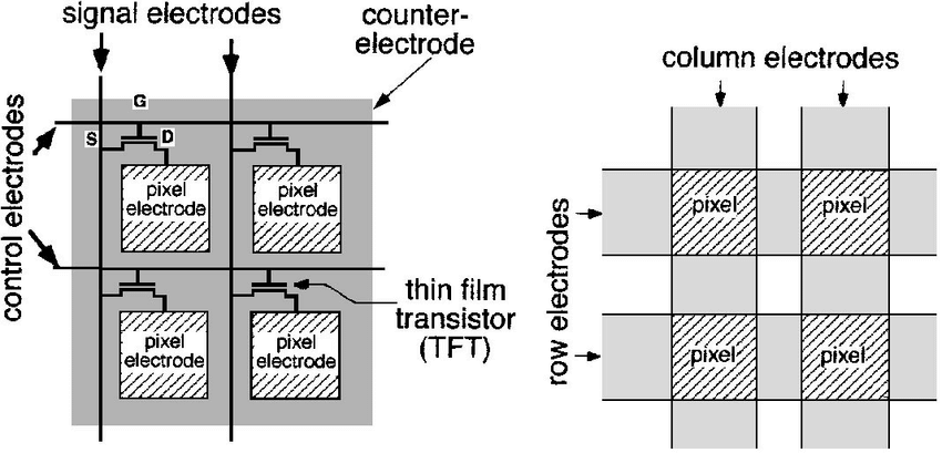
Above, a comparison of the signaling structures of an active-matrix (left) and that of a passive-matrix (right).
Though TFTs can use a variety of materials for their semiconductor layers, silicon has become the most popular, creating the silicon-based TFT, abbreviated as Si TFT. As a semiconductor device, the TFT, as well as all FETs, use solid-state electronics, meaning that electricity flows through the structure of the semiconductor layer rather than vacuum tubes.
Due to the variety in silicon’s possible structures, the Si TFT’s characteristics can vary as well. The most common form is amorphous silicon (A-Si), which is deposited during the first step of the semiconductor fabrication process onto the substrate in low temperatures. It is most usable when hydrogenated into the form A-Si:H. This then significantly alters the properties of A-Si; without the hydrogen, the material struggles with doping (the introduction of impurities to increase mobility of charges); in the form A-Si:H, however, the semiconductor layer becomes much more photoconductive and dopable. The A-Si:H TFT was first developed in 1979 which is stable at room temperature and became the best option for AM LCDs which consequently began rising in popularity after this breakthrough.
A second potential form of silicon is the microcrystalline silicon. Though it retains a similar form to A-Si, this type of silicon also has grains of what is known as crystalline structures. Amorphous structures have a more random, less geometric shape to their network-like structures, but crystalline, on the other hand, is more structured and organized. If grown correctly, microcrystalline silicon has better electron mobility than A-Si:H and greater stability too, as it has less hydrogen within its structure. It is deposited in a similar fashion to A-Si’s deposition.
And lastly, there is polycrystalline silicon, also known as polysilicon and poly-Si. Microcrystalline silicon is the middle between A-Si and poly-Si since poly-Si’s structure is composed of many crystallites. This specific form is made by annealing the silicon material which means adding heat to alter the properties of the structure. With poly-Si, the atoms in the crystal lattice shift and move when heated, and when cooled, the structure recrystallizes.
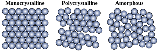
The biggest difference between these forms, notably A-Si and poly-Si, is that charge carriers are much more mobile and the material is much more stable when it comes to using poly-Si over A-Si. When creating complicated and high-speed TFT-based displays, poly-Si’s characteristics allow for this. Yet, A-Si is still very important due to its low-leakage nature, meaning that leakage current is not lost as heavily when a dielectric insulator is not totally non-conductive.
In 1986, the first low temperature poly-Si (LTPS) was demonstrated by Hitachi. LTPS plays a large role in the manufacturing of devices because the glass substrate is not as resistant to high temperatures, so in order to anneal the poly-Si, lower temperatures are used.
Several years later, another development was made in 2012 in the form of indium gallium zinc oxide (IGZO) which allowed for a more powerful display in terms of refresh rates and more efficiency in terms of power consumption. This semiconducting material, as stated in the name, uses indium, gallium, zinc, and oxygen. Though it is a form of zinc oxide (ZnO), the addition of indium and gallium allows this material to be deposited in a uniform amorphous phase but also maintaining the oxide’s high carrier mobility.
As TFTs began to increase their presence in display technology, transparent semiconductors and electrodes became more appealing to the manufacturers. Indium tin oxide (ITO) is an example of a popular transparent oxide used for its appearance, good conductivity, and ease of deposition.

Research of the TFT with different materials has led to the application of threshold voltage, or how much voltage is needed to turn on the device. This value is greatly dependent on thickness and choice of the oxide. When it comes to the oxide, this relates back to the idea of leakage current. With thinner layers and certain types of oxide, the leakage current may be greater, but this in turn could lower threshold voltage, as leakage into the device will also increase. In order to tap into the TFT’s potential for low power consumption, the lower the threshold voltage, the better the device’s appeal.
Another branch of development that stemmed from the TFT is that of organic TFTs (OTFT). First created in 1986, OTFTs usually use solution-casting of polymers, or macromolecules. This device made people hesitant, as it tended to have a slow carrier mobility, meaning slow response times. However, researchers have carried out experimentation with the OTFT because it has potential to be applied to displays different from those that traditional TFTs are used for, such as flexible, plastic displays. This research still continues today. With its simpler processing than traditional silicon technology, the OTFT holds much potential for modern day and future technologies.
TFT Present: Overview
As discussed, the TFT has evolved to become diversely capable of fulfilling the needs of technological advancements. Due to their great imaging properties as well as affordable, low-cost manufacturing, TFT devices and technology have drastically increased in number and purpose since the creation of the TFT.
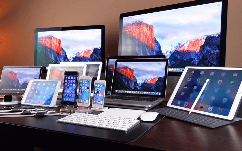
For example, Apple, a well-known and popular brand for a variety of displays, uses the TFT LCD for devices like their iPhones, Macbooks, and iPads. There has been a development that Apple has begun to explore called the organic light-emitting diodes (OLED); OLEDs have the ability to create thinner and more flexible displays. There are still many downsides to this, as of today; the OLED is much more expensive and more fragile to contact with water, so the TFT LCD is still the most prominent display technology in our current time. There is also such a thing as the active matrix OLED (AMOLED), a combination of the OLED layers and TFT layers. This is what Apple has begun implementing in their devices like the iPhone X and Apple Watches. This display allows for deeper, richer colors, something that Apple focuses much of their market on.
But TFT technology and devices are not only limited to displays like those of Apple. With the high resolution and high performance benefits of the TFT, it has found its way into automobile advancement and medical fields. Car dashboards as well as screens often use TFT LCD displays. In medicine, the TFT can act as an image receptor for radiographic images.
As our world now relies so heavily on these sorts of technologies, “technology societies” have emerged to unite engineers, technologists, and other professionals or aspiring people. The Institute of Electrical and Electronics Engineers (IEEE) is one of such and dedicates itself to bettering humanity with technology. A specific subset of this larger group is the Electron Devices Society (EDS) which focuses on electron or ion based devices. This sub-society publishes letters in a scientific journal about theories and designs of electron devices.
The Future of TFT
While there is still room for growth of the traditional TFT, developers have their eyes on expanding the applicative nature of the TFT. Since the 1986 development of the OTFT, the idea of creating flexible displays has been an acknowledged pathway for developers, yet few have chosen this over flat panel displays. These flexible kinds of devices are called large-area electronics (LAE). Using less environmentally toxic materials than traditional TFT displays, LAEs, or more specifically organic LAEs (OLAE), are an emerging expansion for TFT concepts.
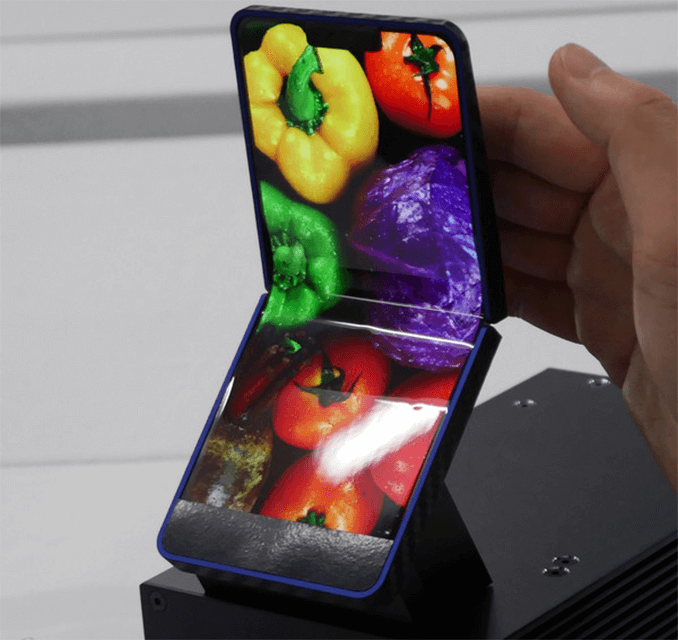
Yet, challenges still present themselves, as these organic displays do not have as many desirable traits that consumers typically want in terms of resolution and response rates. Because of this, traditional TFT LCDs continue to dominate the market, but as research and experimentation on these organic technologies ensue, there has yet to be a limit placed on TFT-based displays, and it is likely that display technology will continue to improve in speed, quality, and versatility.