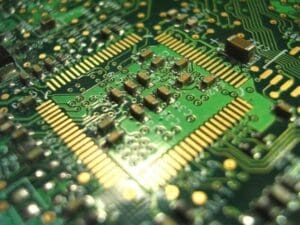
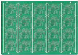
Printed Circuit Board
A printed circuit board (PCB) mechanically supports and electrically connects electronic components using conductive tracks, pads and other features etched from one or more sheet layers of copper laminated onto and/or between sheet layers of a non-conductive substrate. Components are generally soldered onto the PCB to both electrically connect and mechanically fasten them to it.
Printed circuit boards are used in all but the simplest electronic products. They are also used in some electrical products, such as passive switch boxes.
ABOUT US
Orient Display is one of the world’s top-quality PCB (Printed Circuited Boards) manufacturers in the industry. Our PCB factory has 36 years of R&D and production experience, and its annual production capacity is 14 million square feet. We provide customers with PCB technology solutions and supports in customized products for double-sided PCB, multi-layer PCB, HDI, and special PCB such as heavy copper PCB, MMW Automotive Radar PCB, etc. We have experience working in various industries ranging from automotive, appliances, medical, telecom, intelligent terminal, industrial applications, consumer electronics.
Orient Display provides global technical and quality support, guaranteeing a response within 24 hours. We have sales offices in Hong Kong, Seattle, Toronto, and Stuttgart to ensure timely and efficient support for any technical and quality feedback and inquiries. We have a series of advanced PCB manufacturing equipment and a complete quality commitment and certification system( ISO 9001, IATF 16949, ISO 13485, ISO 14001 Environmental Protection, and RoHS Compliant(Halogen free/Lead free)). As a mature company, it takes only 2-3 weeks for sample production and 4-6 weeks for PCB mass production.
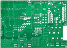
Production Line
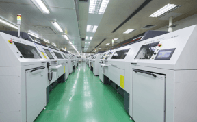
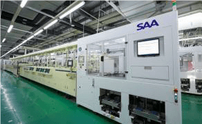
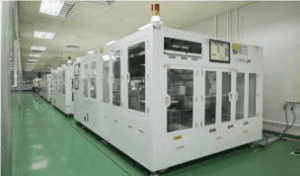
Figure 1. Laser Drilling Figure 2. Bare Board Tester for HDI Figure 3. Vacuum Etching Line
TECHNICAL CAPABILITIES
| Item | Process Capability |
| Max. Multilayer | 32 Layers |
| Inner copper thickness | 0.5 – 6.0 oz |
| Min. line width/ line space | 40/45 (Inner layer)
65/65 (Outer layer) |
| Min. hole diameter
(Mechanical) |
0.15 mm |
| Hole diameter tolerance | ± 0.05 mm |
| Aspect Ratio (PTH) | 16:1 |
| Product size | 730X460mm & 660X558mm (Max.), 50X50mm (Min.) |
| Finished board thickness | 0.20-6.0 mm |
| Board thickness tolerance | T<0.5 mm, ± 0.05 mm,
T≥0.5 mm, ± 10% |
| Min. Distance from PTH to trace | 0.2 mm |
| Min. space between SMD pads for S/M bridge | 50 μm |
| Outline dimension tolerance | ± 0.1 mm |
| Impedance Control | ± 10% |
| HDI (Build-up/ Anylayer interconnection) | 5 +C +5 / 6 +2 +6 |
| Min. hole diameter (Laser) | 75um (3mil) |
| Aspect Ratio (LVH) | 0.9: 1 |
| BGA pitch | 0.35mm pitch |
| Surface finishing | Lead-free HASL, OSP, ENIG, Immersion silver, Immersion Tin, OSP+ ENIG, Gold plating, ENEPIG, Nickel Palladium Plating |
| Material | FR-4
Halogen-free; Lead-free Normal/Middle/High Tg Ceramic board Aluminum substrate Megtron, Nelco, Rogers, Heavy Copper, BT, etc. |
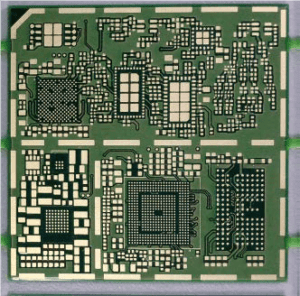
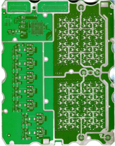
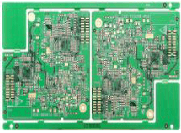
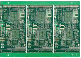
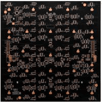
Module PCB
There are mainly two types of module PCB in our company: Internet of things (IoT)/ communication module PCB and vehicle-to-everything(V2X) module PCB.
As the most basic perception layer of the Internet, the IoT/communication module PCB has continued to grow rapidly. Both long-term evolution vehicle-to-everything (LTE-V2X) and new radio vehicle-to-everything (NR-V2X) are important parts of self-driving, the development of the corresponding module board market is increasingly prominent.
| Technical indicator | IoT/communication module PCB | LTE-V2X/NR-V2X PCB |
| Board thickness | ≥0.35mm | ≥0.35mm |
| Stack-up | HDI: 5+C+5; 6 build-up ELIC | HDI: 5+C+5; 6 build-up ELIC |
| BGA pitch | 0.35mm | 0.35mm |
| Min. line width/ line space | 40/40 μm | 40/40 μm |
| μ -via | 75/170 μm | 75/170 μm |
| AR ratio | — | 1.2 |
| Material | EM390, EM526 ,RA555W,
R-A555W,R-A575, EM528K |
S1000-2 ,IT170GRA1,
IT170GT, EM370(D), EM-A50 |
| Core thickness | — | 50 μm |
| Prepreg | 1017 (min.) | — |
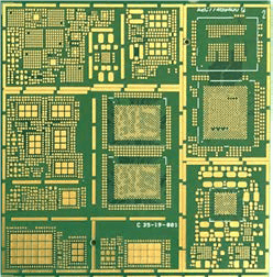
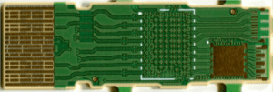
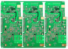
Below figures are LTE-V2X/NR-V2X module PCB.
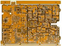
High -Speed PCB
With the development of electronic technology, there is a great demand for high-speed PCB. We have numerous mass production cases, such as:
- Substrate types: Mid loss, low loss, very low loss, and ultra low loss
- The max number of layers: 28; the max thickness: 6.0mm
Special design features: max 3-time compression design, back drilling(including blind hole back drilling) & POFV, the impedance control tolerance≤ 5%, HDI system board, copper inlay, etc.
Our main capabilities are:
- Board size: ≤28*24in, ≤30*20in
- Board thickness: ≤0mm
- Copper thickness: ≤ 6oz
- The stub of back drill: 0.20mm
- AR ratio: 16:1
- Layer to Layer Alignment: ≤5mil
- Impedance: 8%
- Warpage: ≤5%
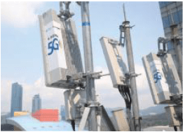
Antenna (5G Sub-6G) PCB
Antenna PCB is widely used in the telecom field to receive and transmit signals. With the development of the 5G network, antenna PCB is perfect for expanding wireless networks and enhancing the broadcasting or receiving stations.
The real cases of production:
- Use ultra low loss high-speed materials(MEG7N) to manufacture RF antenna unit, and the main structures are multi-layer PCB and 2 build-up HDI
- Use ultra low loss high-speed materials to manufacture double-layer microstrip antenna in the 5G mmWave active antenna unit
Our main capabilities are:
- The design of the antenna: Active antenna
- line width/ line space: 40/40 μm
- Board thickness: 0.8 – 1.4 mm
- -via (Laser Via/Pad): 50/140 μm – 75/170 μm
- -via alignment: ≤25 μm
- Stack-up: 12-14 layers; HDI: 5+2+5, 6+2+6
- Surface finishing: ENIG+I-Ag; ENIIG+OSP
- Antenna patch tolerance: 15 μm
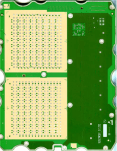
Optical Module PCB
Where there is fiber-optic communication, there is a demand for electro-optical switching modules. The optical module is the key component to realize electro-optical-electro transmission of the signal in fiber-optic communication. We mainly manufacture 100G & 400G high-end high-speed optical modules.
(100G Optical Module PCB)
(400G Optical Module PCB)
Our main capabilities are:
- Board thickness: ≥35mm
- Stack-up: HDI: 5+C+5, 6 build-up ELIC
- Core thickness: 50 μm (min.)
- Copper-inlay: Yes
- Prepreg type: 1017 (min.)
- BGA Pitch: ≥35mm
- Impedance: ± 8-10%
- Warpage: ≤5%
- Laser drilling blind hole: 75/170 μm
- Gold finger: Segmented/ laddered gold finger
- Surface finishing: ENIG, ENEPIG, gold plating (designed area), etc.
- High-speed material: M6, IT968, IT988, EM890K, M7, etc.
Thermal PCB
As the mounting density of SMT increases, the effective heat dissipation area of electronic equipment decreases. Especially when the PCB temperature is greater than 70 , the reliability of the PCB decreases by 5% for every 1 increase. There are three ways of heat transfer: heat conduction, convection and radiation, and all of which are included in the thermal PCB.
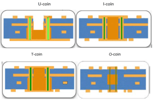
We have CCTC has mass production for 4 types of copper inlay designs:
- Embedded Copper: U-coin, I-coin and T-coin
- Copper Inlayer: O-coin
Our main capabilities are:
- Thermal reliability: Lead-free soldering
- Warpage: ≤75%
- Copper-inlay designs: U-coin, I-coin, T-coin, O-coin, and combined types
- Flatness of joint: ≤ + 2/ -1mil
- Resin remaining on edge of the coin: ≤50mm
Thermal PCB mass production cases (Automotive light & Hybrid vehicle)

4-layer & O-coin & HDI 4-layer & Combined coin & HDI
Heavy Copper PCB
A PCB with a finished copper layer greater than 2oz is defined as a heavy copper PCB. Heavy copper PCB can achieve efficient and reliable power distribution. As a special type of PCB, heavy copper PCB is suitable for high-current capacity products. The significant benefits of heavy copper PCB are that it reduces the chance of circuit failure and enhances the heat transfer from the layer to an external source.
Our main capabilities are:
- inner layer copper: 6 oz
- outer layer copper: 5 oz
- hole copper thickness: 4.5 mil
- Hole copper thickness of other holes (of the same PCB): 0.98 mil
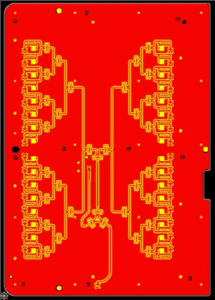
Millimeter Wave (MMW) Automotive Radar PCB
The auto anti-collision radar is the most important part of the developing trends of future automotive technology. MMW radar has advantages in auto-collision avoidance technology.
We have three typical types of auto anti-collision radar:
- 24 GHz SRR (Short range radar)
- 77 GHz LRR (Long range radar)
- 79 GHz MRR (Mid range radar)
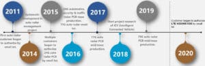
Auto radar development milestones of our company:
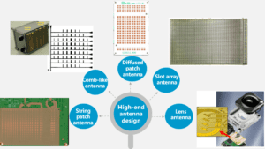
The mainstream designs (mass production) of the antenna at our company are:
- Patch
- Comb-like
- Diffused patch antenna
APPLICATIONS
PCB is widely used in a lot of products, such as Automotive, Power Control units, Medical Equipment, Telecommunications, Consumer products and plenty of other high-tech products.
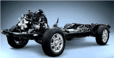
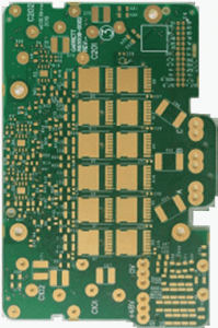
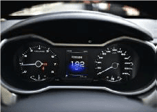
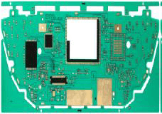
Automotive
Automotive Classis System Brakes (4-layer, TG170, 2oz, ENIG)
Hybrid Vehicle (4-layer, Combined Coin, HDI)
Automotive Dashboard (4-layer, Hole 0.2mm, ENIG)
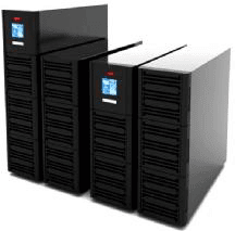
Power Control
Solar Power (4-layer, 2oz, Lead-free HASL)

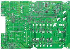
Power Supply (4-layer, TG150, 3oz, Lead-free HASL)
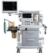
Medical Equipment
Medical Monitor (4-layer, Hole 0.25mm, ENIG)

Medical Breathing Machine (6-layer, Hole 0.25mm, ENIG & Impedance Control)
Telecommunications
Communication (12-layer, ENIG & Impedance Control)
Consumer
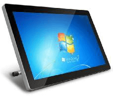
Flat Computer (10-layer, 3/3 mil, ENIG & Impedance Control)
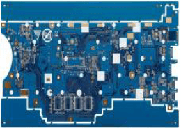
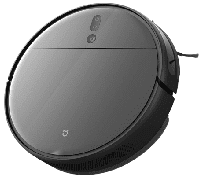
Sweeping Robots (6-layer, Hole 0.2mm, OSP & Impedance Control)
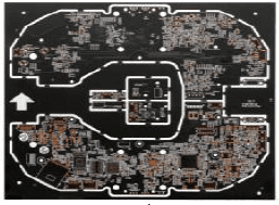
Consumer Electronics (8-layer, Hole 0.25mm, ENIG & Impedance Control)

LED Screen (4-layer, TG150, Hole 0.25mm, OSP)

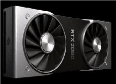
Graphic Card (6-layer, BGA 0.2mm, ENIG+OSP)
CERTIFICATES