What is High Density Interconnector (HDI) PCB
What is High Density Interconnector?
High Density Interconnector is the cutting-edge technology for the production of printed circuit boards. It uses micro-via technology for a printed circuit board with a relatively high wiring distribution density. In other words, HDI PCB is a compact board designed for products with smaller footprint areas. HDI PCB is widely used in cell phones, digital cameras, laptops, automotive electronics, and other digital products.
The advantages of HDI PCB include
- Reduce the cost of PCB, especially the number of layers above 8
- Better electrical performance and signal accuracy
- Improve thermal properties
- Improve radio frequency interference (RFI), electromagnetic wave interference (EWI), and electrostatic discharge (ESD)
What is Micro-Via?
Vias with a diameter of less than 150um or 6mils are called microvias in the industry. In HDI PCB, micro-vias interconnect HDI substrates and printed circuit board layers to adapt to the high input/output (I/O) density of advanced packaging. HDI utilizes this microvia geometric structure technology to make circuits that can improve the efficiency of assembly and space utilization and is also necessary for the miniaturization of electronic products.
Difference between conventional PCB and HDI PCB
Unlike conventional PCB, HDI has not only mechanical drilling for through-hole, blind and buried vias but also laser drilling for micro-vias. High density PCB also has various stack-up arrangements to accommodate micro-vias, thereby diminishing the number of through-holes and inner layers. With the proper arranging of micro-vias, HDI provides better signal integrity and routing space in the inner layers.
High Density PCB Structures
There are mainly two HDI structures:
- Buildup
- Any-layer
Buildup Structure
The buildup structure, which is the basic structure of HDI PCB, uses mechanical drilling as well as laser drilling. Firstly, the core is laminated, drilled by mechanical drilling, plated, and filled. Subsequently, additional micro-via layers are added to the core, and then the drilling, plating, and filling processes are repeated.
N buildup structure has a formula of N+C+N. N and C respectively represent the number of micro-via layers on either side of the core and the core. Figure 1 below shows a 1-buildup structure. It has a through-hole via to connect outer surfaces and another one inside the core drilled before adding HDI layers. Figure 2 below shows a 2-buildup structure of HDI. In the 2-layer of high-density interconnection, stacked micro-vias are copper-filled.
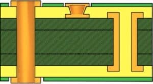
Fig.1: 1-Buildup HDI (1+C+1)
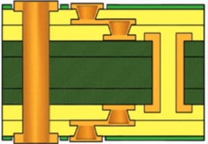
Fig.2: 2-Buildup HDI (2+C+2)
Any Layer Interconnection Technology
Any layer interconnection technology is an advanced technology used in HDI PCB design. It is mainly for high-level interconnection applications since any of the two layers in the PCB can be interconnected without any restriction. In other words, any-layer technology has higher flexibility in the layout, which saves the PCB space at least 30%. However, due to its complexity regarding technology, the cost is higher than conventional buildup boards.
Unlike the buildup structure, the micro-via is first drilled in the layer by laser drilling, followed by repeating processes of copper plated, inner-layer image transfer and press, and the outer-layer imaging transferring finally. Figure 3 below displays the general flow chart of any-layer technology. It is worth noting that the diameter of micro-vias and the thickness of prepregs are both less than 4miles.
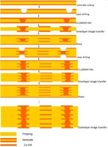
Fig. 3: The Flow Chart of Any Layer Technology
Take a 3+2+3 any-layer structure as an example ( Figure 4 below). CO2 laser drill machine is used for drilling. The micro-vias are realized by via copper filling technology, which fills copper through vertical continuous plating line(VCP) and horizontal plate line.
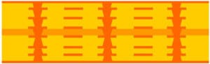
Fig. 4: 3+2+3 Any Layer HDI PCB
Reference:
https://www.protoexpress.com/blog/becoming-a-pcb-master-hdi/
Check Also: Types of PCB.