
I2C is the most commonly used communication protocol in CTP systems. When customers report touch issues, we often use an oscilloscope to verify whether the CTP is functioning properly. Understanding how to analyze I2C waveforms is therefore essential for problem diagnosis and effective technical communication with customers.
Background of I2C
I2C (Inter-Integrated Circuit) was originally developed by Philips in 1982 for communication between its internal chips. The original specification supported speeds up to 100 kHz with 7-bit addressing. Although 7-bit addressing allows up to 128 addresses, some are reserved, so only 112 valid device addresses can be used on a bus.
In 1992, the first public specification introduced 400 kHz Fast Mode and extended 10-bit addressing. In many systems (for example, Arduino-compatible boards using the ATmega328 microcontroller), I2C support typically remains at Standard Mode (100 kHz) or Fast Mode (400 kHz), with either 7-bit or 10-bit addressing. Higher-speed modes (1 MHz to 5 MHz) exist but are less common.
*Serial vs Parallel Communication
Serial communication (e.g., I2C, UART, SPI, USB) transmits one bit at a time over a single data line in time sequence.
Data for I2C is typically as:
Clock
1 0 1 1 0 0 1 0 // I2C will transmit these data one bit by one bit
Parallel communication (e.g., MCU parallel bus, RGB interface) transmits multiple bits simultaneously in one clock cycle.
Data for RGB is typically as:
D7 D6 D5 D4 D3 D2 D1 D0
1 0 1 1 0 0 1 0 // 8 bits are transmitted in one clock cycle.
I2C Bus Architecture
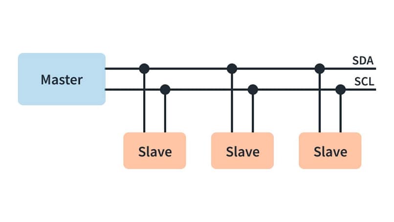
I2C supports multi-master and multi-slave configurations and operates in half-duplex mode.
Customers often mention the term “node.” A node refers to any device connected to the I2C bus that has a valid address and is capable of communication. A node can function as either a master or a slave device.
A slave device, such as our Touch IC, cannot initiate communication. It can only respond to requests from the master. The slave must recognize its own address and will respond only when the received address matches its configured address.
For example, assume three slave devices have addresses 0x1A, 0x2A, and 0x3A. When the master transmits 0x2A on the SDA line, the second slave compares the received address with its own. If the address matches, communication is established.
Although all slave devices can detect the address transmitted by the master, only the device with the matching address will respond by sending an ACK (0). The others will ignore the transaction (NACK = 1). Each device address must be unique and is typically determined by hardware configuration. Examples will be provided later.
Half-duplex means that data can flow in only one direction at a time — either from master to slave or from slave to master. The data direction is controlled by the R/W bit.
In the I2C bus, SCL is the clock line and is always generated by the master. SDA is the data line and uses an open-drain structure, meaning it can be pulled low by either the master or a slave device.
Open-Drain Structure
What is an open-drain (or open-collector) structure? This type of output driving method enables bidirectional communication on a single data line in I2C systems.
An open-drain output can actively pull the signal line low or remain in a high-impedance (Hi-Z) state, but it cannot actively drive the line high. In contrast, a push-pull output can actively drive the signal either high or low.
When multiple devices are connected in parallel on the same bus, push-pull outputs may cause signal conflicts or even short circuits if different devices attempt to drive the line to opposite logic levels at the same time.
Push-pull output uses complementary PMOS and NMOS transistors to determine whether the output drives a high level (VDD) or a low level (ground).
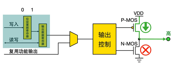
High Level
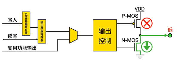
Low Level
In an open-drain output structure, the PMOS transistor is permanently turned off (disconnected).
The circuit can either drive a low level (when the NMOS is turned on and conducts) or remain in a high-impedance state (when the NMOS is turned off).

Low Level
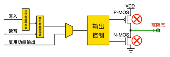
High-impedance state
When an external pull-up resistor is connected, the value of the pull-up resistor will appear at the output. PN-MOS itself are two diode2, with essentially infinite resistance.)
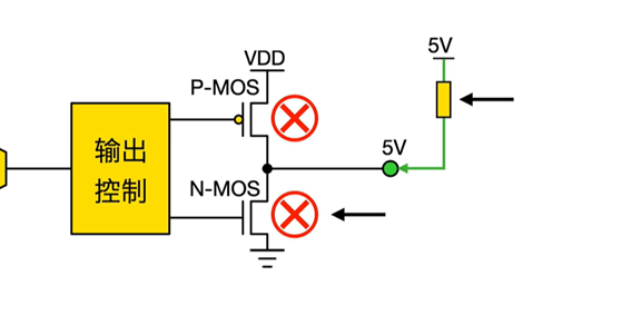
Open-Drain structure with a pull-up resistor
Only after understanding what open-drain outputs and pull-up resistors are can we better interpret the waveforms of SCL and SDA. In theory, SCL should be a regular square wave with very clean rising and falling edges.
In practice, for normal SCL and SDA waveforms, the falling edge is fast and sharp because the pull-down is active. The rising edge, however, is slower and curved or sloped because the voltage is pulled up through a resistor charging the line’s capacitance
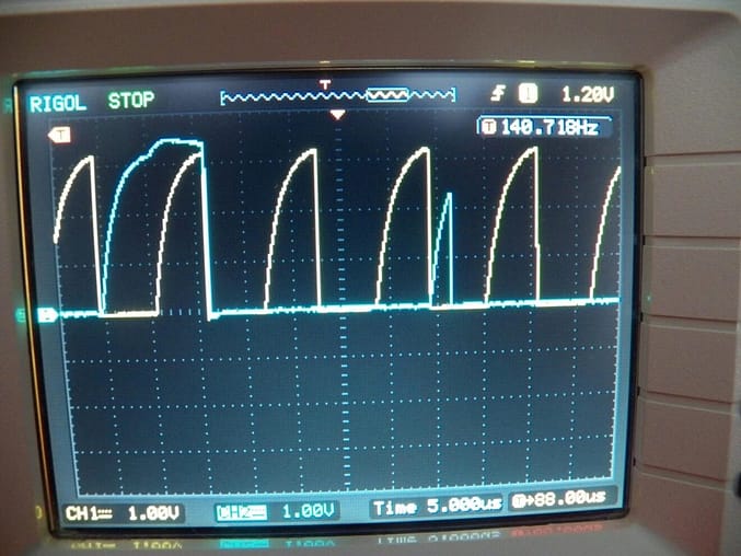
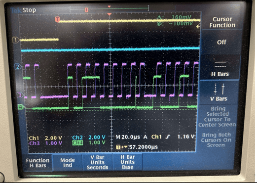
As in the photo above, the yellow SCL line has a very slow rising edge, which is usually caused by a pull-up resistor that is too large.
Generally, for 100 kHz I²C, a 4.7 kΩ pull-up resistor is recommended, and for 400 kHz, 2.2 kΩ. If the pull-up resistor is too large, it can sometimes cause the touch sensor to become unresponsive.
A smaller pull-up resistor results in faster rising edges and stronger noise immunity, but it also increases power consumption.
I2C Data Format
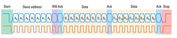
Start and Stop Conditions
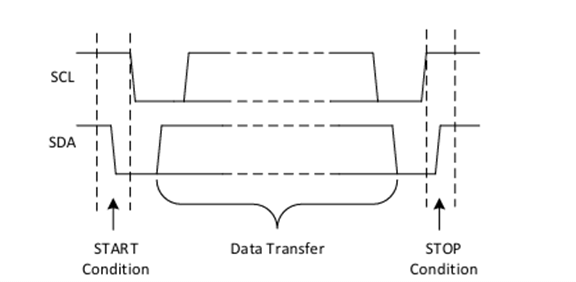
When SCL is high: SDA transitioning from high to low indicates a START condition; SDA transitioning from low to high indicates a STOP condition.
Addressing
An address frame typically consists of a 7-bit address plus 1 R/W bit (0 = write from master to slave, 1 = read from slave to master).
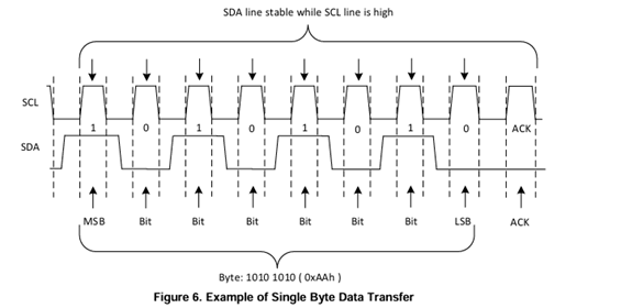
SDA must change only when SCL is low. During SCL high, SDA must remain stable because data is sampled during the high period of SCL.
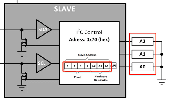
In the diagram below, we can see that the slave’s A1, A2, and A3 pins are all connected to ground. This makes the address 1110000, which is 0x70 in hexadecimal.
Some devices, however, do not have A1, A2, and A3 address pins. In that case, the address cannot be changed and is fixed as a default internal static address.
ACK / NACK
After every 8 bits of data, the 9th clock cycle is used for ACK/NACK. The receiver drives SDA: ACK = 0 (acknowledge), NACK = 1 (not acknowledged).
A short pulse may appear between the 8th bit and the ACK bit. This occurs when the SDA line is released during direction switching. Because this transition happens while SCL is low and data is sampled during SCL high, this short pulse is not interpreted as valid data.
If you have any questions, please contact our engineering.