
Key Reasons for ESD Requirements for Displays Becoming Increasingly Common
-
Electronic Components Are Becoming More Precise and Sensitive
As technology advances, the internal components of displays—such as integrated circuits (ICs), driver chips, and touch panels (TP)—are becoming more miniaturized and low-power. This makes them less tolerant to electrostatic discharge (ESD), where even a small static charge can cause functional abnormalities, shorten the lifespan, or directly damage the components.
-
Applications Are Becoming More Diverse and Complex
Display usage has expanded beyond traditional indoor environments to more demanding settings, such as:
- Industrial equipment: frequent friction and dust accumulation easily generate static electricity
- Medical devices: require high reliability and safety
- Automotive systems: enclosed environments easily lead to electrostatic induction
- Outdoor terminals: dry climates increase the risk of static charge build-up
-
Widespread Use of Touch Technology
As touch displays become more common, users frequently interact directly with the screen. In dry environments or when wearing synthetic fabrics, it is easy to generate static electricity. Discharge directly onto the touch surface poses a greater risk to circuit integrity, so enhancing surface-level ESD protection is essential.
Our standard TFT displays typically meet the following ESD protection levels:
- Air discharge: ±8KV
- Contact discharge: ±4KV
These are in line with the specifications described in our datasheets and are essential for ensuring product reliability.

-
With increasing application demands and evolving environmental challenges, higher Electrostatic Discharge (ESD) protection levels are often required for display modules
particularly in industrial, automotive, and outdoor settings. When customers request enhanced ESD performance, such as:
- Air Discharge: ±15KV
- Contact Discharge: ±8KV
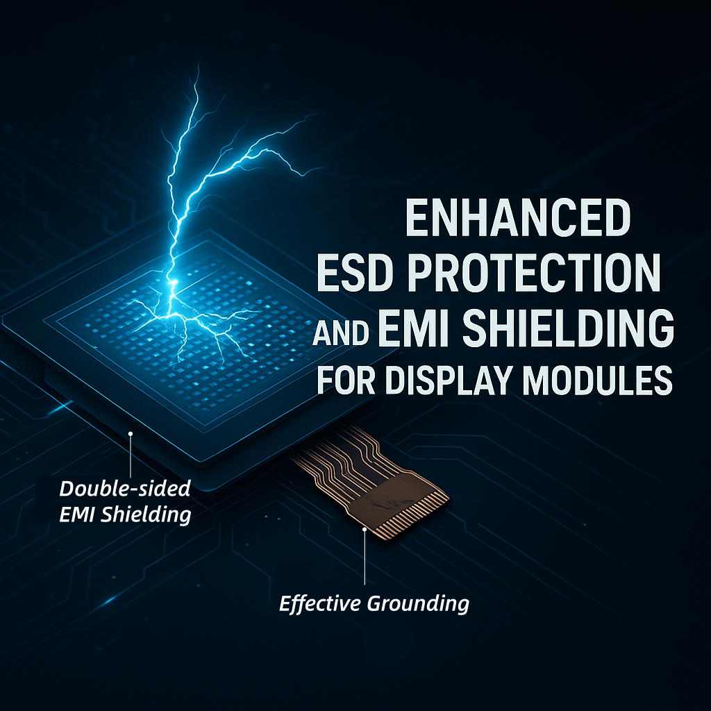
Recommended Solution: Double-sided EMI Shielding
Component: FPC Shielding Layer
Structure: Double-sided EMI (Electromagnetic Interference) Shielding Film
Description:
To improve the Electromagnetic Compatibility (EMC) of the display module, we recommend the use of a Double-sided EMI shielding structure. This design involves applying EMI shielding materials to both the front and back sides of the display module.
Key Functions:
- Effectively suppresses internal and external electromagnetic interference
- Enhances the stability and reliability of signal transmission
- Helps meet higher ESD immunity levels as specified in IEC 61000-4-2 standards

Additional Recommendations
In addition to the EMI shielding layer, further system-level measures can be considered
- Grounding design optimization between module and enclosure
- Use of conductive foam or gasket around the module perimeter
- Application of anti-static coatings or films on exposed surfaces
EMI shielding material is like an “umbrella” that blocks interference.
Grounding wire is like a “drainpipe” that channels interference away.
Only by combining both can we achieve a true “shielding + discharge” integrated protection.
Examples of Common Grounding Methods:
| Application Area | Grounding Method |
| LCM metal backplate | Connected to the mainboard GND point |
| Touch FPC shielding layer | Grounded via GND pin or metal frame |
| Conductive foam/tape | Attached to grounding copper foil or metal housing |
| EMI shielding sticker | Connected to grounding point on housing or bracket |
Signal Ground vs. Chassis Ground
Although both are referred to as “ground,” Signal Ground and Chassis (Physical) Ground have different purposes and characteristics in electronics:
Signal Ground (Logic Ground)
Purpose: Serves as a voltage reference for signal transmission (typically 0V)
Location: Internal circuit ground used by ICs, resistors, capacitors, etc.
Characteristics:
-
- Used in logic and analog circuits
- Not necessarily connected to the earth
- Typically found in low-noise, low-current environments
Example: The GND pin of an MCU or sensor
Chassis Ground / Earth Ground
Used once the display module is integrated into the full device
Purpose:
-
- Discharge static electricity (ESD) to prevent component damage
- Reduce EMI via housing-level shielding
- Improve EMC performance through unified grounding
Example: Metal frame, conductive tape, or backlight housing grounded to the device chassis
Summary
To meet elevated ESD requirements (±15KV air / ±8KV contact), both EMI shielding and effective grounding are essential.
By combining signal-level reference grounding with chassis-level discharge pathways, and by incorporating double-sided EMI shielding, we can ensure robust protection, greater product reliability, and compliance with industrial EMC/ESD standards.
Does your project have special requirements for ESD protection? Feel free to contact our engineer at <tech@orientdisplay.com>—we’re always happy to help.